
Around the world, a great deal of effort is being put into nanofabrication and the development of new lithography methods, with the result that feature sizes of less than 100nm can now be readily generated. However, as features get smaller, these top-down methods become increasingly complex and costly. Alternative methods to create structures on the nanoscale based on (molecular) self-assembly might offer several advantages, such as even smaller feature size, more material flexibility and reduced cost.
These bottom-up methods have the potential to extend the microelectronics roadmap and allow the continued reduction of feature sizes, as Moore’s law suggests. But their potential application reaches far beyond microelectronics.
Go deeper with GlobalData

Discover B2B Marketing That Performs
Combine business intelligence and editorial excellence to reach engaged professionals across 36 leading media platforms.
Many material properties – optical, mechanical, biological and others – are influenced by the nanoscale topography of surfaces, opening the way to applications in biology, chemistry and materials science in general. And here, it is not necessarily a disadvantage that self-assembly only usually allows periodic or quasi-periodic structures to be generated.
BUILDING ON POLYMERS
Using polymers as building blocks for self-assembly is interesting for several reasons. First, polymers come in a wide variety of properties, varying in size, chemistry or functional group, and they are often biocompatible or even biodegradable. Further, they show various phenomena that can lead to the creation of nanoscale patterns. Also, many of them can be produced in economically viable ways.
Micrometre scale patterns can be readily generated from polymers by demixing binary polymer blends during spin-coating. This phase separation process is similar to the separation of oil and water and produces quasi-periodic patterns with characteristic shapes and sizes.

US Tariffs are shifting - will you react or anticipate?
Don’t let policy changes catch you off guard. Stay proactive with real-time data and expert analysis.
By GlobalDataThe resulting structures depend on the polymers used and their concentration, as well as on the solvents, spinning speed and other experimental factors. By careful adjustment of all these parameters, a whole range of morphologies, with feature sizes typically in the micron range, can generally be obtained.
Clearly, these demixing structures of two different polymers influence the chemistry of the surface, and they offer ways, for example, of modifying the surface-wetting properties. By changing the demixing behaviour over small lateral length scales, gradients of surface chemistry can be created over distances ranging from a few millimetres to a few centimetres.
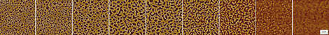
Large gradients offer a wide range of surface energies concentrated in a small area, and are interesting in screening applications, such as for cell growth and adhesion studies (see Figure 1).
Instead of being used as is, the demixed polymer film can be treated further. In a subsequent step, one of the polymer constituents can be removed by using a selective solvent, leaving behind a microporous film with a large internal surface. When added to the chip surface of conventional optical biosensors, for example, increased detection sensitivity could be reached due to larger specific binding in the detection region.
ON THE NANOSCALE
Patterns considerably smaller than one micrometre can be created with polymeric self-assembly, if the non-mixing constituents are chemically bound to each other. These block copolymers show effects, similar to demixing, called microphase separation, which describes the ordering of identical building blocks into microdomains. Since the polymeric entities are covalently linked to each other, the separation length is restricted and the typical length scale of the resulting pattern is molecular.
In the case of the di-block copolymers that we typically use at the Swiss Center for Electronics and Microtechnology (CSEM), this corresponds to some 30–50nm. Again, the size and the spacing of the resulting patterns strongly depend on the molecular weight of the polymeric blocks, solvents used, and other experimental parameters. This allows us to control their properties to some extent.
Combining both polymer demixing and microphase separation is straightforward and provides access to complementary length scales, creating structures ranging from some 30nm up to 10 microns, all by molecular selforganisation.
And if a purely random though quasi-periodic structure is not sufficient, then other patterning methods might be combined in order to direct self-organisation into the desired direction.
More and more researchers are becoming active in the field of templated self-assembly. Considering all its advantages, polymeric self-assembly represents an attractive toolbox-like approach to micro- and nanostructures. Its flexibility and its use of fairly standard materials, combined with low-cost instrumentation, make it very interesting for applications.
WHAT’S GOOD FOR CELLS?
For certain applications, a larger variety in surface topography is needed than polymer self-assembly can deliver. CrN films made by plasma vapour deposition (PVD) show a wide range of different morphologies; again they can be nicely controlled by the experimental parameters during deposition.
At CSEM, we have produced films composed of crystallites which are vertically elongated needles, cubes or pyramids, and morphologies that look more like tiny vegetables. These surfaces are hard and very resistant to wear. We have started using these surfaces for cell studies, in order to characterise their influence on cell growth and adhesion (see Figure 2).
Comparative studies were performed on smooth chromium nitride films and films with pyramidal crystallites of different sizes. Despite identical surface chemistries, very different cell behaviour took place on the surfaces:
• A smooth surface gave good cell adhesion and proliferation.
• Crystallites larger than around 200nm gave very poor adhesion and proliferation.
• Small crystallites exhibited intermediate behaviour.
In part these effects can be understood as being the result of the exceedingly sharp edges of the pyramidal crystallites.
TINY DROPLETS AT WILL
Despite the high flexibility of the self-assembly processes described above, the disadvantage remains that these structures are random in nature. In those cases where a precise localisation of a nanometric structure is required, lithographic methods with highly precise placement capabilities are required. Advanced lithography and electron beam direct writing have pushed the feature size to below 100nm for thin films and solid materials known from microfabrication.
A novel method that allows the deposition of tiny amounts of liquids is based on scanning force microscopy (SFM). An SFM probe with a tiny aperture at the tip apex is brought into contact with the substrate surface, and some attolitres of liquid are transferred from the tip reservoir to the surface through the aperture (nanoscale deposition, NADIS, see Figure 3).
Careful adjustments to the surface energies of both substrate and probe are necessary in order to optimise the amount of liquid that is deposited. The probes are prepared either by microfabrication – similar to what is commonly done for SPM probes – or by focused ion beam (FIB) modification of commercially available SPM probes. The deposited liquid can be used to transport molecules in solution or particles in suspension, or it can be a liquid precursor material.
As an example of solvent deposition, and to show a combination of bottom-up self-assembly with top-down methods, the opening of copolymer micelles by NADIS deposition of selective solvents is shown in Figure 4.
Like many other advanced SPM methods, NADIS is not particularly user-friendly and rather slow. Current work aims at delivering the liquid from distant reservoirs to the dispensing tip through dedicated nanochannels, and to operate many of these NADIS probes in parallel. Although NADIS is still in the development stage, its potential is clearly visible. We are currently investigating its application to create tiny protein arrays.
Self-assembly and advanced scanning probe methods offer interesting possibilities, in particular in the biomedical field. More time has to be spent for a complete understanding of the processes involved and to better control the experimental parameters, but the first applications have started to appear.