
US Photonics
Research, Development and Testing of Medical Components and Devices
Subscribed
You have successfully submitted your enquiry. Someone from our company will respond ASAP
About Us
US Photonics undertakes research, development and testing of medical components and devices. We specialize in microfluidics, laser micro-machining, sensors, exotic materials, coatings, and prototyping.
US Photonics is geared to be an a la carte research and development facility for corporations, companies, and inventors who either do not have resources in-house to allocate to a project, or who do not have the required facilities and or equipment in general. We have also been know to be the last bastion of hope for projects thought to be too impractical or all-out impossible, as we have a track record of succeeding where others have given up or failed.
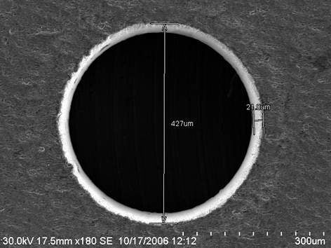
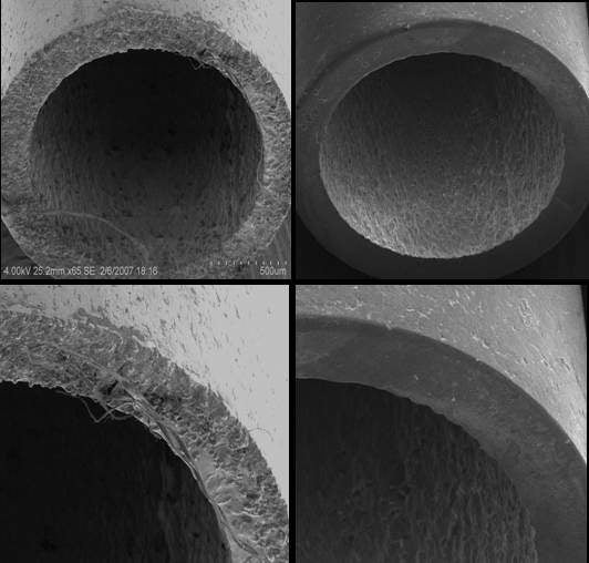
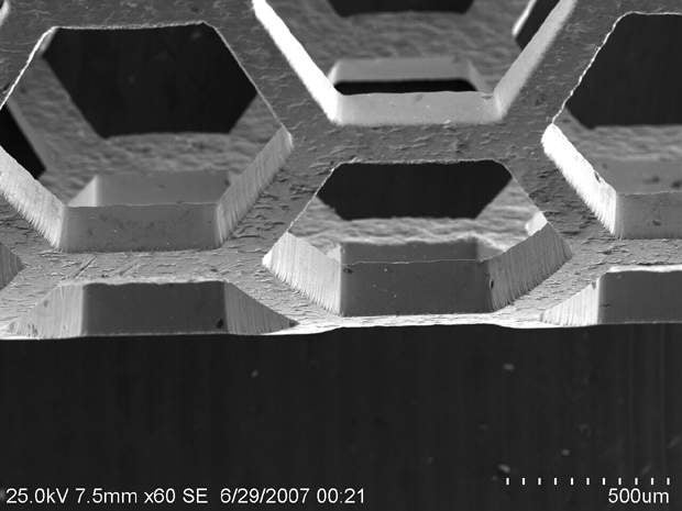
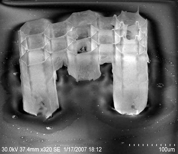
Microfluidics devices
US Photonics can create virtually any pattern in any material used in microfluidics applications, including glasses, tissues, polymers, diamond, carbides, nitrides, and stainless, with micro and nano-sized features possible. We specialize in prototyping, one-offs, and short runs of microfluidics devices, along with creating tooling and systems for mass production.
Laser micro machining
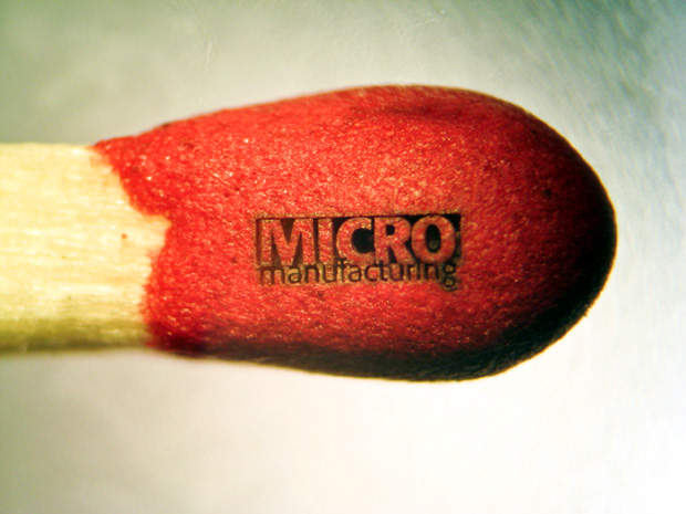
The ultra-fast femtosecond laser technology used at US Photonics affords us some very crucial advantages over other state-of-the-art laser types. The most notable advantage is the lack of heat transfer during the ablation of a material, which avoids the thermal damage associated with traditional machining techniques (laser, EDM, hard tool, etc.) and has the ability to cleanly ablate materials that would otherwise melt, crack or fracture, and even has the ability to ablate highly flammable materials such as the head of a match. This level of precision allows us to selectively remove nanometer-scale thin films from a substrate without damage to the underlying substrate.
Our five-axis micro/nanomachining center boasts a 20nm following error with up to 200mm/s speed with 150mm travel (X/Y), 360° continuous rotation on two axes, and 100mm Z axis travel. It also utilizes a photolithographic mask imaging system with an axial 6.6MP camera with confocal microscope-based real-time surface profiling and autofocus.
Sensors for data collection and analysis
Knowledge is power, and in life-threatening situations having up-to-the-minute information is critical. Sensors that collect data and have it analyzed on the fly save time and lives. We can create sensors that remove the delay between sample taking and having that sample analyzed in a lab. Fiber-optic, chemical, spectroscopy, optics, microfluidics, and electronics are some of the avenues that we use to create custom components and whole systems, which are used to gather, compile data, and alert end users when conditions are changing.
We also create custom-fit software to read and gather the raw data so that it can convert it into interpretable information for the end user.
Exotic materials research and development
Many of the research and development projects we are involved in allow us to become very familiar with a wide range of exotic materials, which are at the forefront of many emerging technologies. Some of these include but are not limited to advanced polymers, carbon nano tubes (CNTs), nitinol, quantum dots, solgels, and aerogels.
We are also familiar with taking well-established materials into the nano realm, which are showing alternate and exciting properties not usually associated with the material while it is comprised of the larger, traditional particle sizes.
Medical device coatings
From thin film deposition, sputter and spin coating, electrophoretic deposition, electrospray / electrospinning, dip coating, CVD and pulsed laser deposition (PLD) for use in optics, sensors, circuits, etc., US Photonics can accommodate multiple facets of coatings.
Medical device prototyping
Whether it is a quick prototype resin printing, multiphoton polymerization, a CNC machined component, or a laser CNC micro/nano machined part, we are ready to bring new ideas to life. With the aid of advanced software such as Solidworks 2010 and ComsolMultiphysics we are able to virtually build prototypes and even test them in the computer before ever producing a physical part, saving time, resources, and money.
Power systems for medical devices
From hand-held instruments and battery backup UPS to micro power cells and implantable devices, our drive is to continue to make smaller, more powerful, and ultra-reliable power sources that can recharge faster with fewer thermal issues and maintain greater stability. Through the use of nano-sized materials and state-of-the-art chemistry, our battery technology has the potential to revolutionize portable medical devices, and give freedom to some devices currently deemed too power hungry for portability.
Contact Details
Website
Email Address
Address
Missouri 65806,
Springfield,
Other,
United States of America