
Wearable electronic medical devices are changing the way people manage their health. Remote patient monitoring (RPM) devices used by patients returning home from hospital lets health practitioners closely, yet remotely, monitor their patient’s post-operative recovery and watch for any complications.
Other patients with long-term and chronic illnesses incorporate convenient health monitoring within their daily lives without the need to attend regular office visits by wearing small, discreet devices. They track real-time results such as blood glucose levels, body temperature and blood pressure to help detect irregularities before they turn into dangerous health problems. Many often connect to smartphones for easier readings.
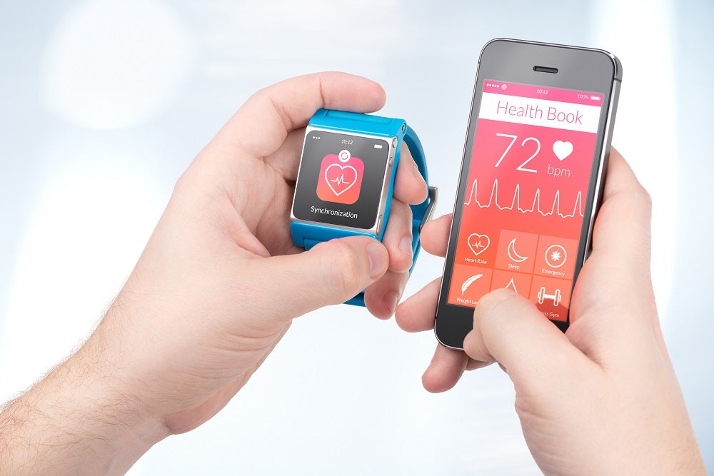
Others rely on fitness trackers and smartwatches to measure exercise levels and calorie intake or to analyse their sleep patterns to support healthier lifestyles. Wearable electronic devices are also used to monitor loved ones and summon assistance in the event of a fall or medical emergency.
The challenge of producing clean, small devices
As wearable electronic medical devices get more complex and powerful, the challenge is to keep them small, discrete and comfortable for patient wear. This means the internal printed circuit boards (PCBs) that power the devices must shrink too.

Wearable medical devices are typically densely packed with tiny, multi-layered PCBs. The PCBs often have bottom termination components, such as ball grid arrays (BGAs), chip-scale packages (CSPs), micro leadframes (MLFs), quad-flat no-leads (QFNs) and Decawat Packages (D-Paks). These are low clearance or zero clearance, making it difficult to clean and rinse away contaminants like solder balls, active flux or flux residue from under them. Other common production contaminants that must be removed are marking inks, fingerprints and simple dirt and dust.
Contaminated or dirty PCBs, if not properly cleaned prior to device assembly, are susceptible to a number of problems. These include parasitic leakage, electrochemical migration, delamination, dendrite growth and shorting. All of these can lead to faulty, unreliable performance or even catastrophic field failure.

Choose a cleaning method
There are a number of ways to clean PCBs, from benchtop manual cleaning to in-line aqueous operations. As PCBs become more challenging to clean, however, medical device manufacturers are turning to vapour degreasing as a tested and proven cleaning method. Vapour degreasing is a simple thermo-mechanical process that boils and condenses a specially-engineered low-boiling non-flammable cleaning fluid to remove PCB contaminants.
Vapour degreasers use a closed-loop system containing two chambers, the boil sump and the rinse sump. The boil sump contains a low-boiling, non-flammable cleaning fluid. The PCBs are immersed and cleaned inside the heated fluid. Once cleaned, the PCBs are mechanically transferred to the rinse sump for a final rinse and dry in more pure, uncontaminated fluid, or inside the fluid vapours themselves. The PCBs come out clean, dry and spot-free. The process is simple, repeatable and easy to validate.
Choose the right cleaning fluid
What is really transforming vapour degreasing for the medical sector is the advancement in solvent technology. Environmentally progressive modern cleaning fluids can substantially enhance the electronics and completed device performance, reliability and longevity.
Many modern PCB cleaning fluids used inside the vapour degreaser have exceptional materials compatibility, making them suitable for cleaning delicate plastic parts or mixed-material printed circuit boards. They also have low surface tensions and high liquid densities. This allows the cleaning fluid to easily flow around tight-fitting and low-mounted components to clean under them thoroughly. It also enables the fluid to flow back out from under the components, preventing the fluid and the contaminants from getting trapped. This ensures all contaminant is completely removed.
The safer alternative to aqueous cleaning
Unlike the widely-used aqueous systems, vapour degreasing uses no water. Water is a natural breeding ground for bacteria and mould, as are some of the detergents used with it. This means bioburden control is an ongoing issue when cleaning devices with any water-based system. Even a minuscule amount of moisture in hard-to-reach areas can encourage the growth of bacteria. If it is not properly addressed, moisture can result in increased complications during product validation.
For this reason, some medical device manufacturers are turning to solvent-based cleaning fluids that are inimical to pyrogens, minimising bioburden risk. Vapour degreasing also reduces the possibility of bioburden contamination because assemblies come out clean and dry enough for immediate coating or packaging.

Meet manufacturing cleanliness standards
Wearable medical electronics, as well as the PCBs used in them, must conform to strict regulatory guidelines when it comes to design, manufacturing and certification. Quality, predictability and safety are all priority concerns for the sake of patients and medical staff, as well as for the hospital and product manufacturers who are liable.
There are a number of International Organisation for Standardisation (ISO) requirements to follow, including ISO 10993. This evaluates devices within a risk management framework to ensure they are safe, assessing bioburden, pyrogens and sterility to ensure that no harmful material remains on the device and that the device is safe for its intended use.
Another benchmark standard is IEC 60601-1. Specified by the International Electrotechnical Commission (IEC), this regulation is explicitly designed for medical electrical equipment and systems, necessitating that the basic safety and essential performance of the medical device must be maintained. PCB cleaning is a central practice to help to meet this requirement.
Find a cleaning partner
Wearable medical devices continue to gain popularity as people become more proactive in monitoring their health. As wearable electronic medical devices get smaller and more complex, cleaning their internal PCBs becomes more critical to ensure they perform without fail.
By choosing a trouble-free cleaning method and modern cleaning fluid, device manufacturers can be well-prepared to produce clean, reliable PCBs. Vapour degreasing helps eliminate bioburden, offers an easy way to validate the manufacturing process and meets the stringent regulatory criteria used in the medical device manufacturing industry.
Before deciding on a method or fluid, consult with a Microcare critical cleaning applications expert. They specialise in cleaning fluids designed specifically for the medical sector. They can suggest compatible and effective cleaning fluids for compliance as well as device reliability and longevity.
Go to microcare.com for more information or contact us to discuss how the right cleaning fluids and methods can help you produce clean and reliable PCBs.
Author information: Emily Peck is a Senior Chemist at MicroCare, which offers benchtop and vapour degreasing electronics cleaning solutions. She has been in the industry for more than six years and holds an MS in Chemistry from Tufts University. Peck researches, develops and tests cleaning-related products that are used on a daily basis in electronics, medical and precision cleaning applications.
