DYCONEX: Discovering a World of Excellence
Based in Switzerland, DYCONEX engineers and produces printed circuit boards, operating at the leading edge of the high-density interconnect and micro-via segment.
DYCONEX specialises in interconnect solutions for implantable medical devices, avionics, aerospace and scientific equipment
You have successfully submitted your enquiry. Someone from our company will respond ASAP

DYCONEX AG, headquartered in Bassersdorf near Zurich, Switzerland, is a global leader in the design and manufacture of highly complex printed circuit boards (PCBs), with a specialization in high-density interconnect (HDI), flexible, rigid-flex, and biocompatible substrates for medical and scientific applications. With over four decades of experience, DYCONEX has established itself as a premier supplier to OEMs and research institutions that require customized, miniaturized, and reliable interconnect solutions. The company has built a reputation for quality, innovation, and precision, underpinned by its Swiss roots and a deep commitment to customer-specific solutions.
DYCONEX was founded in 1991 following a management buyout from Oerlikon-Contraves, but its roots trace back even earlier to technology developments within the Swiss electronics and defense industry. Since its foundation, the company has continuously expanded its technological capabilities and service portfolio. Today, DYCONEX is part of the SOMACIS Group, a renowned global PCB manufacturer. This integration has further strengthened DYCONEX’s position by allowing access to complementary technologies, manufacturing capacity, and global customer support.
The company has always maintained a strong focus on demanding applications, particularly in the field of medical technology. Over 90% of DYCONEX’s business is in the medical sector, and it has long-term relationships with many of the world’s leading medical device manufacturers. Additionally, DYCONEX serves customers in scientific instrumentation, industrial automation, and other niche applications that require precise, reliable, and miniaturized circuit solutions.
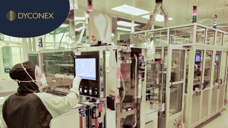
Through consistent investment in research and development, state-of-the-art production equipment, and the ongoing training of its workforce, DYCONEX continues to set new standards in PCB technology. The company operates a modern facility that includes cleanroom production environments and a highly skilled interdisciplinary team of engineers, chemists, physicists, and technicians.
DYCONEX offers a wide range of high-end PCB solutions that are tailored to the most demanding applications. Its core products include:
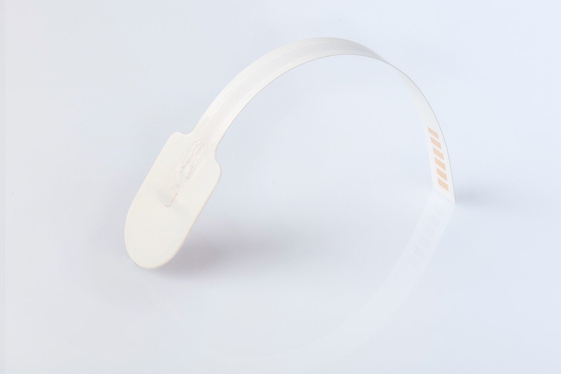
Flexible PCBs
Flexible printed circuit boards are used in devices that require high-density signal routing in compact or dynamic environments. DYCONEX’s flex PCBs offer multi-layer construction, ultra-fine lines and spaces, and high aspect ratio vias, enabling compact and lightweight end-products. The achieved reliability of the flexible printed circuit boards is one of the key strengths and enables the use in medical and challenging environments.
Rigid-Flex PCBs
These combine the benefits of rigid and flexible substrates, making them ideal for complex three-dimensional designs. DYCONEX provides rigid-flex PCBs with custom stack-ups, optimized for durability, space-efficiency, and reduced connector requirements.
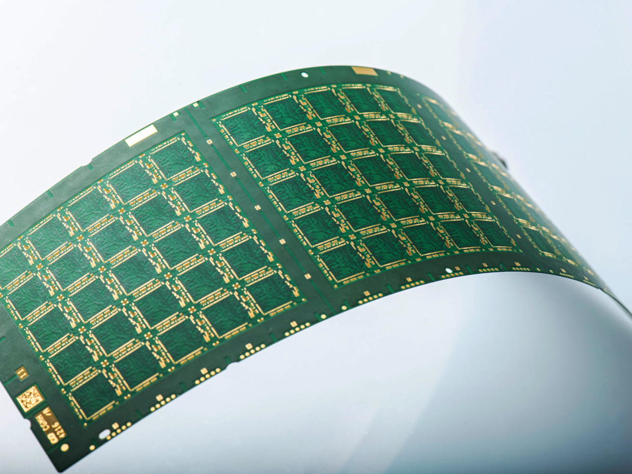
Ultra HDI Substrates
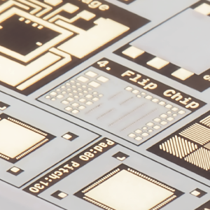
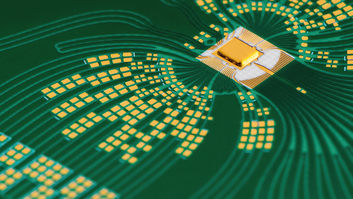
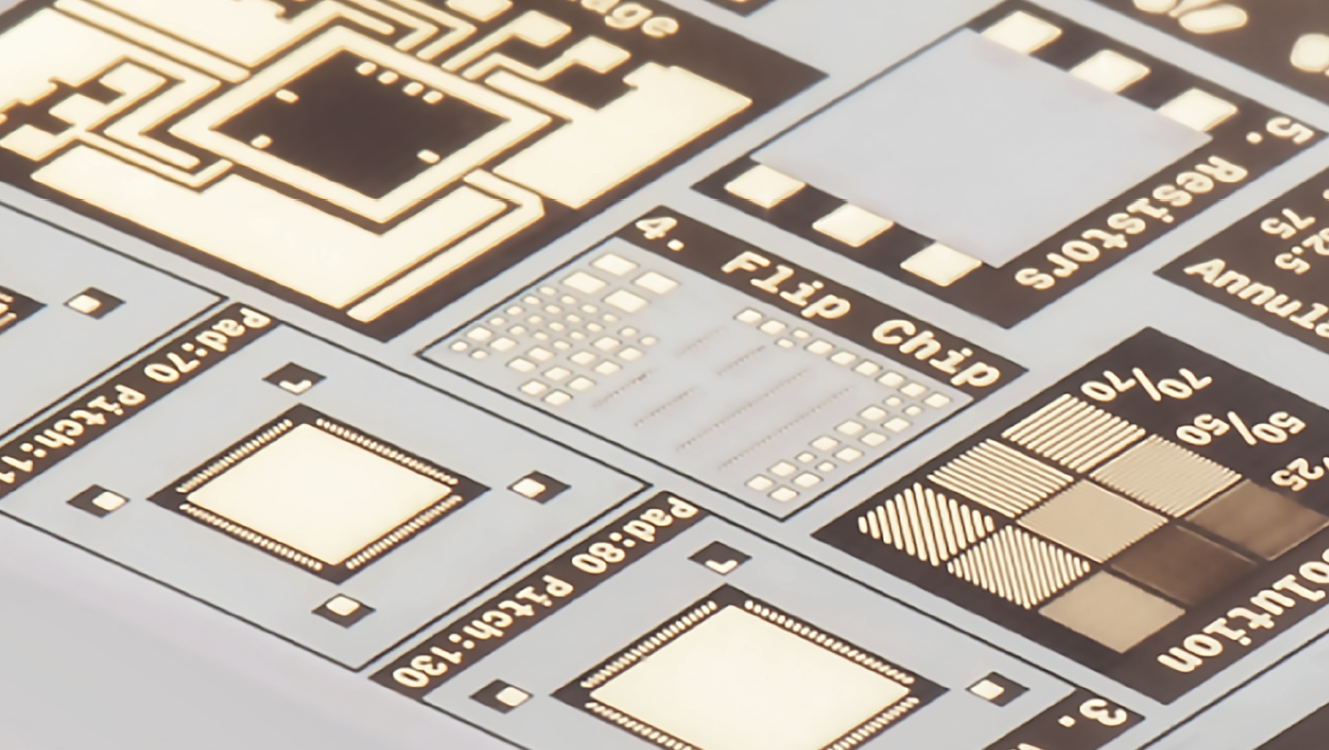
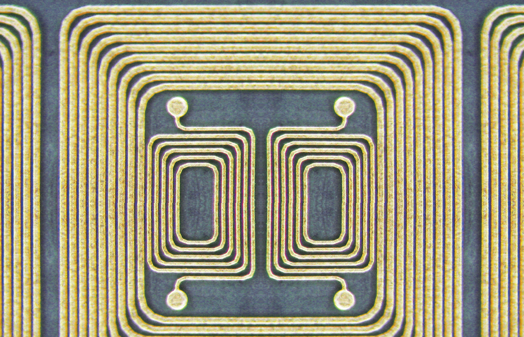
DYCONEX has developed and industrialized ultra-high-density interconnect substrates with features such as line/space down to 8 microns, laser-drilled microvias, and fine-pitch BGA support. These are used in applications where size, weight, and electrical performance are critical.
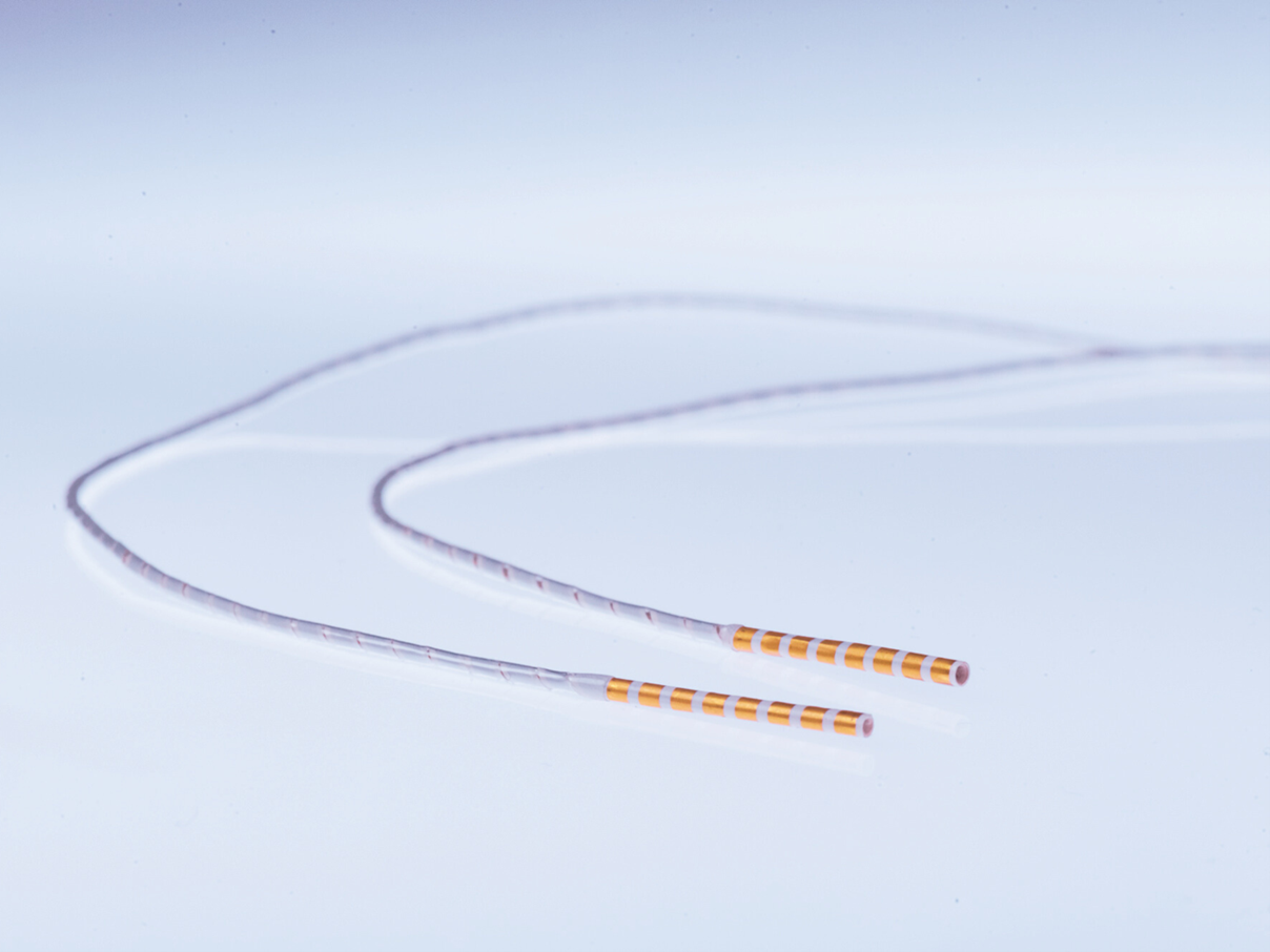
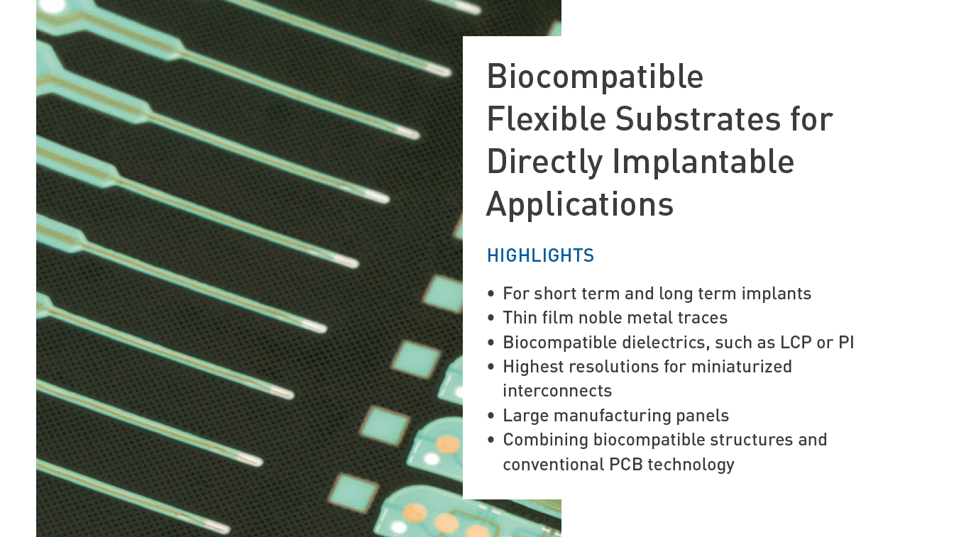
Implantable Substrates & Electrodes
Specializing in biocompatible materials and surface treatments, DYCONEX provides substrates for implantable devices including neural interfaces, cardiac implants, and active hearing devices. Products are customized for shape, thickness, flexibility, and longevity.
Custom Solutions
Many of DYCONEX’s products are developed in close collaboration with customers, resulting in highly customized interconnect solutions with unique mechanical, thermal, and electrical properties.
DYCONEX’s technology portfolio encompasses some of the most advanced PCB processes available today:
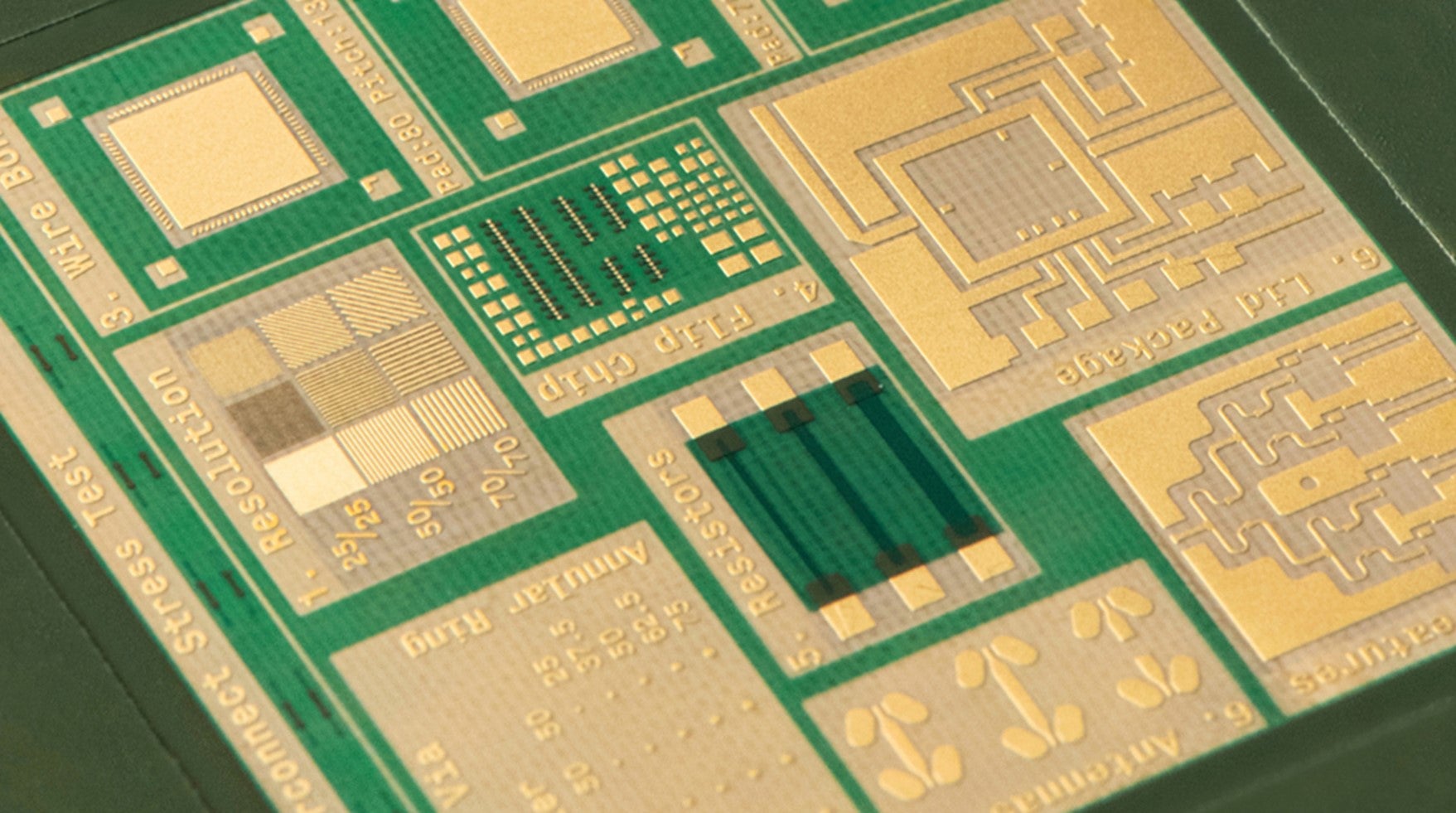
High-Density Interconnect (HDI)
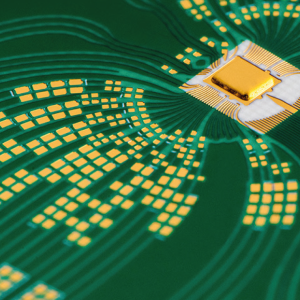
DYCONEX was an early adopter of HDI technology and continues to refine these processes for medical and scientific use cases. The company’s HDI capabilities include microvia technology, via-in-pad structures, stacked vias, and ultra-fine lines/spaces.
Semi-Additive Process (SAP)
Using advanced SAP and mSAP techniques, DYCONEX achieves exceptional trace definition and layout accuracy. This is essential for next-generation medical implants and high-frequency circuits.
Laser Direct Imaging (LDI)
High-resolution LDI systems enable precision patterning for HDI and flex-rigid PCBs. This improves yield, registration accuracy, and the ability to support dense component placement.
Biocompatible Materials
DYCONEX works with a wide range of medically approved materials including polyimide, LCP (Liquid Crystal Polymer), and other specialty films. These are selected based on their flexibility, durability, and chemical stability in biological environments.
Cleanroom Manufacturing
Cleanroom production lines ensure particle-free manufacturing environments, a necessity for producing substrates used in implantable devices and high-reliability electronics.
Microfluidic & Diagnostic Structures
The company is also active in producing microfluidic PCBs, often used in scientific and diagnostic applications. These incorporate micro-channels, fluidic ports, and integrated electronics in one compact platform.
DYCONEX’s products are used in critical applications where failure is not an option. Key market segments include:
Medical Devices
The dominant market for DYCONEX. Applications include:
Scientific Equipment
Used in high-precision analytical systems, lab-on-chip platforms, and microfluidic diagnostic equipment. These require tight tolerances, stable performance, and often biocompatibility.
Industrial & Semiconductor
DYCONEX serves a select group of industrial customers needing high-reliability, miniaturized electronics for automation, sensing, and control. Also includes substrate solutions for advanced semiconductor packaging.
Innovation is at the heart of DYCONEX’s business model. The company actively participates in international research consortia, such as iNEMI and Medtech Europe, and collaborates with academic institutions to push the boundaries of what is technically feasible.
Continuous investment in R&D has resulted in proprietary processes for microvia reliability, electroplating, surface finishing, and adhesive-free lamination. These advances translate directly into higher performance and reliability for the end-user.
DYCONEX maintains a comprehensive quality management system. With ISO 9001 and ISO 13485 certification, the company ensures its processes comply with the most rigorous standards. For implantable devices, every step of the manufacturing process is traceable. Statistical process control, automated optical inspection, electrical testing, and accelerated life testing are all part of the company’s standard quality workflow.
The commitment to quality is also reflected in DYCONEX’s internal culture. Continuous improvement programs, training, and cross-functional teams ensure that quality is embedded at every level.
DYCONEX offers its customers a broad range of engineering services that span the entire product lifecycle:
Design for Manufacturability (DfM)
The company supports customers during the early design stages to ensure optimal manufacturability, cost-efficiency, and compliance with application requirements.
Stack-up & Material Consulting
Advising on material selection and layer stack-up configuration is a key part of DYCONEX’s value proposition, especially for medical and scientific products where biocompatibility and stability are critical.
Prototype to Series Transition
From small batches for testing to full-scale series production, DYCONEX ensures process continuity and scalability.
Failure Analysis & Testing
The company offers analytical services, including cross-sectioning, SEM analysis, and electrical testing to identify issues and validate designs.
Regulatory Support
For medical customers, DYCONEX assists with documentation and testing required for regulatory approval, including FDA and CE conformity.
DYCONEX sees itself not just as a supplier, but as a development partner. Regular design reviews, co-development workshops, and dedicated technical support are part of the customer journey.
DYCONEX AG is a pioneer in high-end printed circuit board technologies with a strong focus on applications where performance, reliability, and miniaturization are mission-critical. As part of the SOMACIS Group, it combines the high-quality of a specialized Swiss manufacturer with the global capabilities of an international player. Whether it’s powering a life-saving medical implant or enabling the next breakthrough in diagnostics, DYCONEX delivers engineered solutions that meet the highest standards of technology and trust.
Based in Switzerland, DYCONEX engineers and produces printed circuit boards, operating at the leading edge of the high-density interconnect and micro-via segment.
Introducing our advanced thin film technology featuring electroplated pure gold traces, vias, and pads. With a platinum surface finish for electrodes, this material is thin, highly flexible, and bio-stable for long-term implant use.
For Highly Durable and Reliable Miniaturized Electronics
High Reliability and Component Density for Advanced Electronics
Ultra-Fine Structures for Maximum Density and Performance
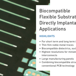
This white paper describes DYCONEX’s biocompatible, flexible LCP/PI-based substrates with embedded noble-metal (gold) thin-film traces and optional electrode coatings (Pt, PtIr, IrO2, Ti) for high-resolution, glue-free, short- and long-term implantable applications such as sensors, catheters, neurostimulation leads, and implantable electrodes.
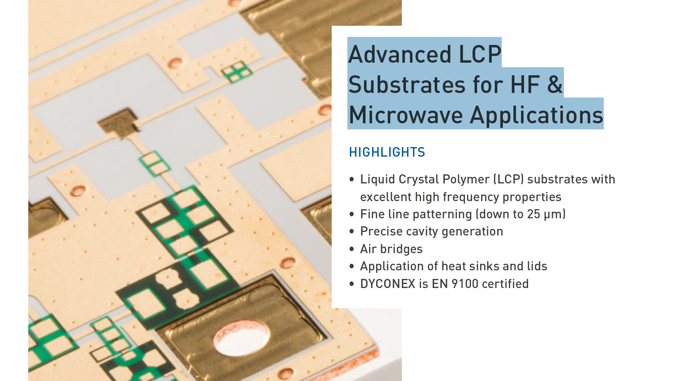
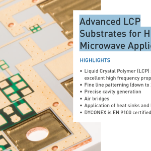
Dyconex’s liquid crystal polymer (LCP) multilayer substrates deliver low-loss, moisture-stable, high‑frequency performance up to 100 GHz with fine-line patterning (≥25 μm), laser blind vias, thermal vias and metal lids/inserts for efficient heat dissipation, ENEPIG gold‑wire bondability, and options for near‑hermetic, high‑temperature, high‑power-density packages.
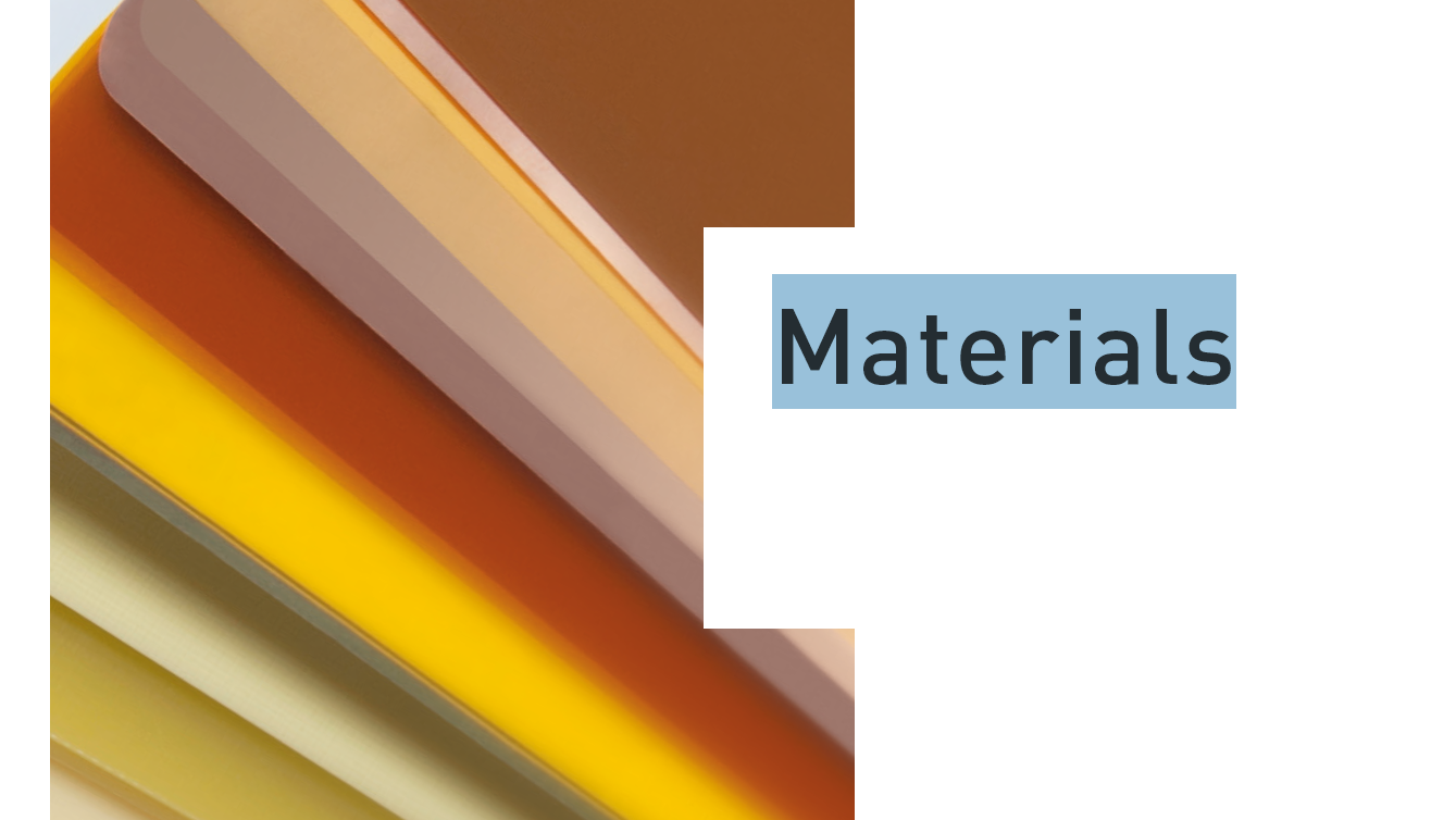
This white paper provides a comprehensive, up-to-date reference of Dyconex PCB materials — including rigid, flex and rigid‑flex substrates, adhesives, constraining layers, surface protection and finishing options — tailored for high‑reliability, high‑frequency and advanced interconnect applications.
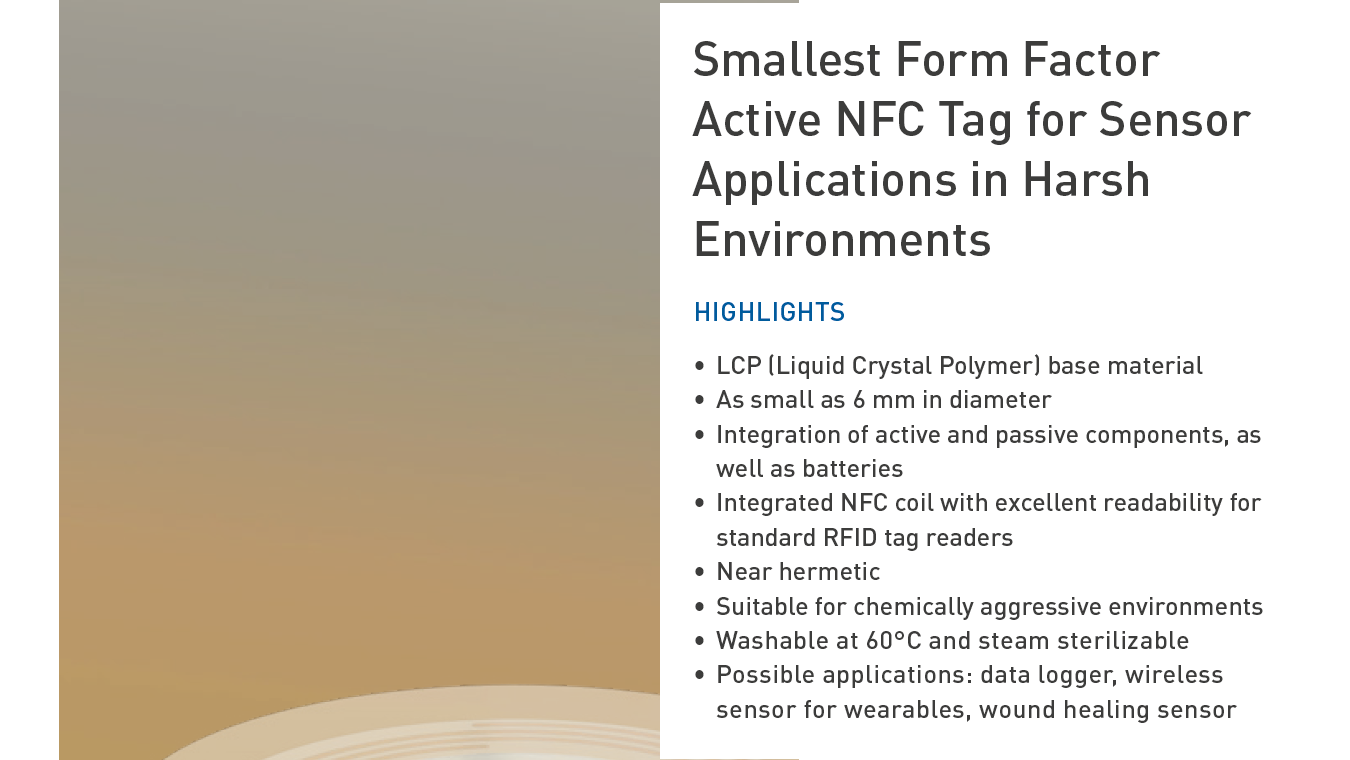
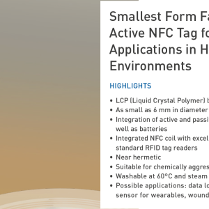
A 6 mm-diameter, 2.5 mm-thick active NFC sensor module encapsulated in liquid crystal polymer (LCP) that integrates battery, ASIC, sensor and NFC coil for reliable, near-hermetic operation in chemically aggressive, washable and steam-sterilizable environments up to 150°C.
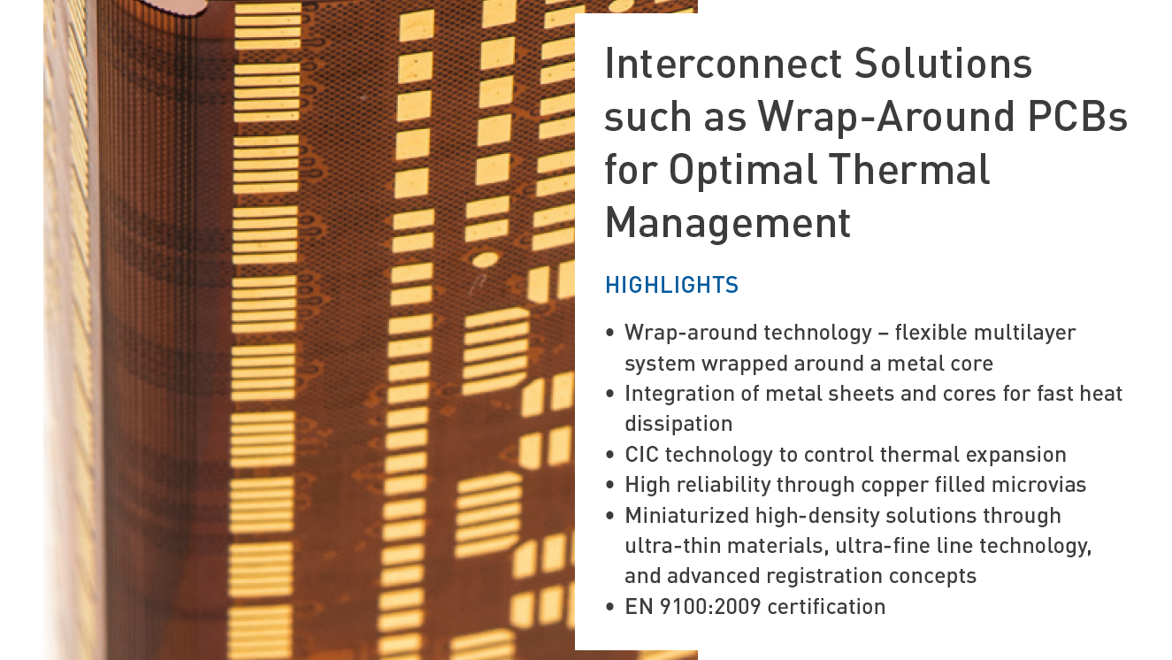
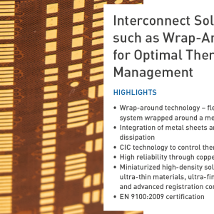
A concise white paper presenting DYCONEX's wrap-around PCB interconnect solutions—combining flexible multilayer circuits, copper-filled microvias, metal back-sheets/cores (CIC, CMC, Al) and advanced materials (LCP, polyimide)—to separate electrical and mechanical functions and deliver high-density, highly reliable thermal management for aerospace, defense, and RF applications.
Dyconex will be exhibiting at this year’s MDM Minneapolis, October 21–22, at booth #3137. The company will highlight its latest capabilities and innovations for implantable flexible printed circuit boards (PCBs) and advanced miniaturization.

Discover how flexible PCBs enable high‑reliability, biocompatible medical devices – from implantables to ultra‑compact systems – while meeting the strictest performance and materials requirements.
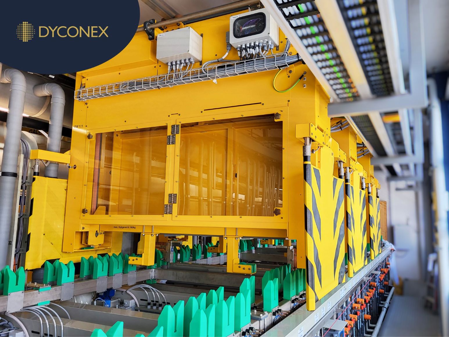
With this key technology upgrade, we are expanding our capabilities and taking an important step forward in high-precision PCB manufacturing.
Our LCP solutions are setting new standards in miniaturisation and reliability for medical implants.
This line also features DYCONEX-developed technology that significantly improves the reliability.
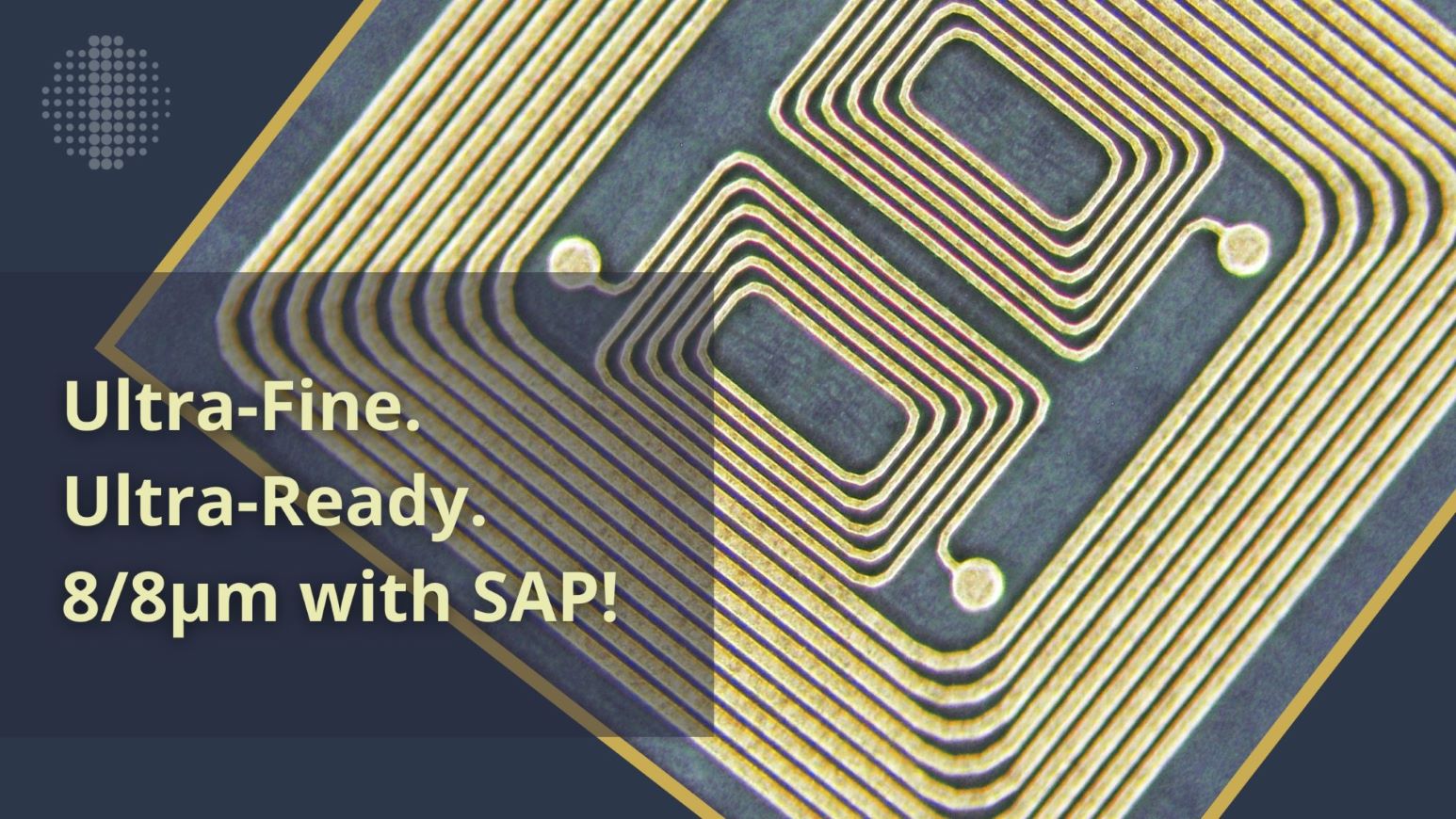
SAP is revolutionising PCB production, offering even smaller features, enhanced precision, and better control over copper thickness.
Pushing the limits of flexible PCB technology.
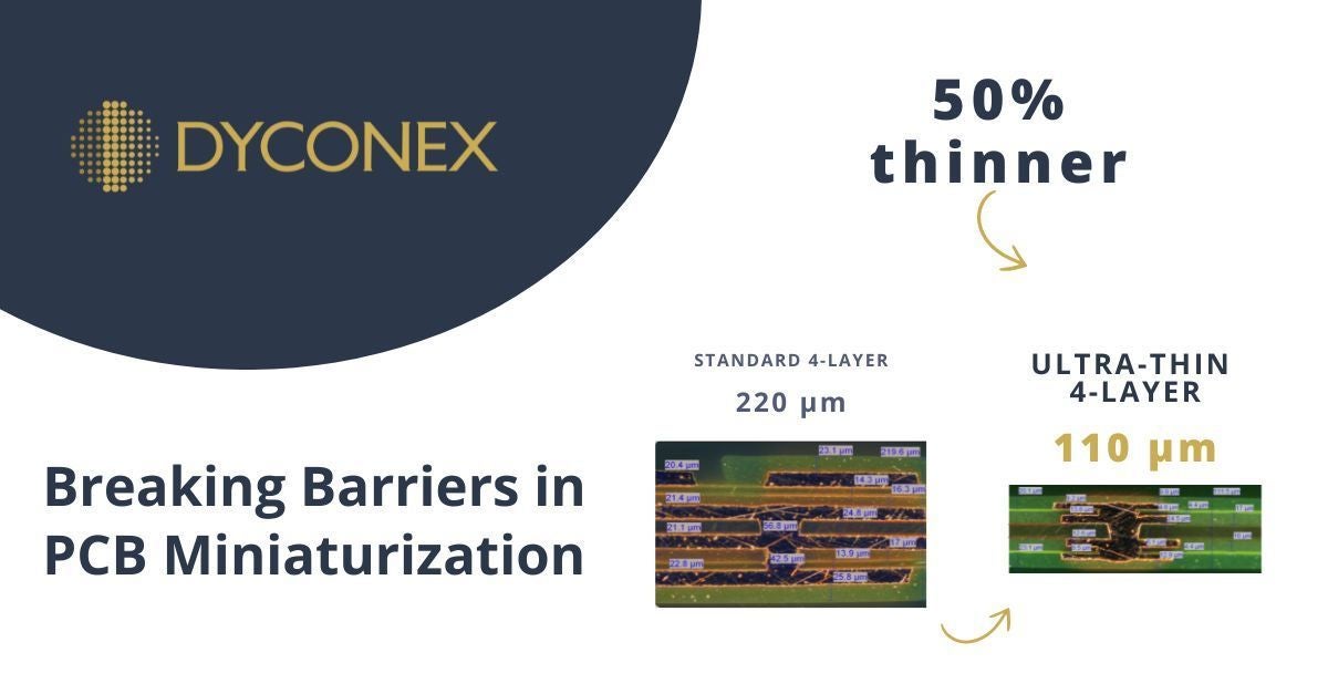
The future of flex PCBs is thinner, more flexible, and more durable than ever.