
MedTech-Revolution: AT&S Accelerates Innovation Through Testing and Simulation
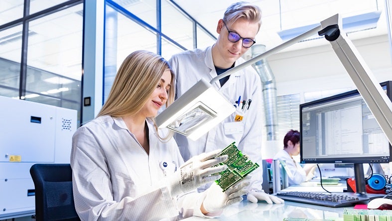
AT&S offers its sophisticated engineering services to customers in the medical sector, speeding up development cycles without sacrificing reliability.
AT&S supplies printed circuit boards and other electronic interfaces for the development of medical devices.
You have successfully submitted your enquiry. Someone from our company will respond ASAP

AT&S supplies printed circuit boards (PCBs) and integrated circuit (IC) substrates to companies worldwide, with medical devices being one of our key industries. We have been active in the industry for more than 30 years and currently employ more than 15,000 colleagues.
We aim to stand out from other PCB suppliers through our passion for innovation, broad and flexible technology setup, and dedicated service and support for our partners.
AT&S has partnered with medical device companies for more than ten years, developing and promoting new PCB technologies for their products.


Our operations are supported by a dedicated medical team consisting of business development and engineering experts worldwide. The team is familiar with the special requirements of the medical device industry and passionate about driving innovation and enabling solutions.
Our partners choose to work with AT&S because of our process knowledge and efficiency, as well as our ability to scale innovation and technological leverage between customer segments. We produce PCBs of the highest quality through our experience in IPC Class III, offering various test and qualifications standards.
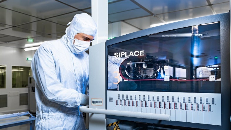
AT&S operates six production facilities worldwide, these facilities enable us to develop PCBs quickly from the prototype stage to serial production, with a strategic focus on high-end technologies and applications combined with an ISO 13485-certified quality management system.
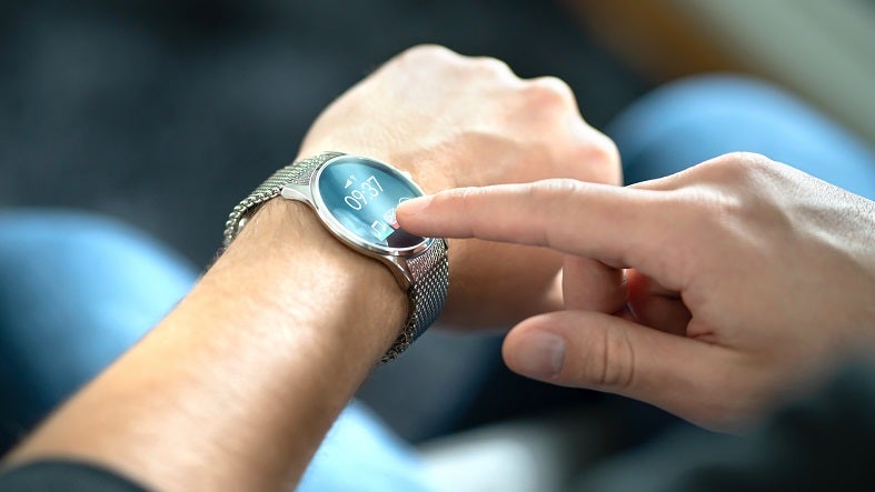
Products that use AT&S solutions include cardiac bionics, hearing aids and cochlear implants, neuromodulation, wearables, diagnostic and imaging, catheters, prosthetics, and drug delivery systems.
AT&S provides cutting-edge technologies to enable the latest developments in the medical industry. We develop for and in partnership with our customers to meet their individual requirements and give them an edge over their competitors.
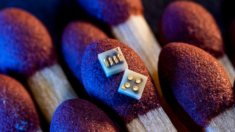
A particular focus for us is in miniaturisation, which is playing an increasingly large role in the field of medicine. From implants such as cardiac pacemakers and neurostimulators to hearing aids and wearable monitoring systems, high-end medical applications are becoming smaller to increase patients’ comfort as much as possible. This requires additional, more powerful components to enable new features and increase the functionality of these devices.
Below is a short overview of AT&S’ technology portfolio:
AT&S understands that the medical market is constantly changing and innovating amid trends such as e-health and digitalisation, with consumers paying more attention to their health and seeking new devices to meet their needs.
Working in partnership with our clients, we draw on our broad technology portfolio and innovations in other sectors to develop the most suitable solution for customers’ needs. Our manufacturing process covers both prototype and series production, ensuring fast and smooth development cycles.
AT&S provides high-end PCBs and IC substrates for the mobile device, automotive, industrial, and medical sectors. Initially founded via a merger of several state-owned Austrian firms, the company was privatised and sold in 1994 and has since begun trading on the Vienna Stock Exchange.
We currently operate six production facilities in Europe and Asia, with each facility focusing on a different technology portfolio. The research units at our plants in Shanghai, China, and Leoben, Austria, play a key role in advancing technology within the AT&S Group.
AT&S offers its sophisticated engineering services to customers in the medical sector, speeding up development cycles without sacrificing reliability.
Be it implantable devices such as pacemakers or neurostimulators, hearing aids or portable multi-parameter monitoring systems: high-end medical applications have to become smaller and smaller to make life as comfortable as possible for patients.
The Styrian technology company continues its expansion offensive and expanded its plant in Ansan, Korea, where high-quality interconnect solutions for medical technology are produced.
Established in 2022, the Innovation Award Styria honours the best projects of Styrian companies and research institutions. The prize is awarded by the Styrian Business Promotion Agency SFG in cooperation with the Department of Economic Affairs of the Province of Styria. Around 100 Styrian companies and institutions took their chance in the competition of the best and applied with their projects. With an innovative solution for miniaturised, flexible printed circuit boards, AT&S was able to claim the premiere victory in the digitalisation category.

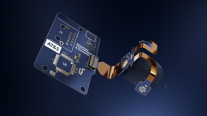
New design options and miniaturisation with attractive designs for all ages thanks to our flexible PCBs with increased functionality at smaller sizes.

Bring components within the PCB to create more space for batteries with higher capacity, and make patients safer by limiting the risk of external influences.
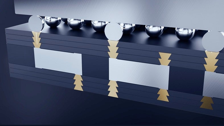
Harness the power of microchips with IC substrates from AT&S - the interface between the world of semiconductors and PCBs.
High-tech for your applications, HDI printed circuit boards have played an important role in the history of AT&S; indeed, they marked the beginning of the company’s rise to become the market leader in the manufacture of high-end PCBs.

Multilayer PCBs consist of several layers, are space-saving and ensure fast connections between components with up to 28 layers from electronic shielding to high-frequency variants.

Better hearing without interference thanks to the best sound processors powered by AT&S module PCBs for increased comfort by connecting hearing aids to entertainment devices.

Intelligent heat management for your devices, and power management in electric vehicles with faster charging thanks to thermal management in our PCBs. Our printed circuit boards promise optimal performance, even at high temperatures.

Improve your signal integrity and speed with clear and fast communication without signal loss, and transfer large quantities of data wirelessly to enable autonomous driving and machine-to-machine communication.