Multilayer PCBs

The basis for new innovation in electronics.
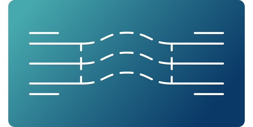
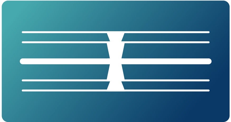
Multilayer PCBs consist of several layers, are space-saving and ensure fast connections between components with up to 28 layers from electronic shielding to high-frequency variants.
Multilayer printed circuit boards are AT&S’s core business and form the basis for most technologies used for further miniaturizing electronic circuits and systems. At the dawn of modern electronics, printed circuit boards were simple resin-bonded paper with circuits printed on one side. But technology soon developed in response to increasing demands for integrating and miniaturizing electronics.
Multilayer PCB benefits:
- Multilayer printed circuit boards ensure short and fast signalling pathways.
- The layered structure allows for complex circuits.
- The compact design enables further miniaturisation of circuits and devices.
Today, AT&S can produce printed circuit boards with four to 78 layers, which can be adapted to almost all system manufacturer requirements. Multilayer printed circuit boards have contributed to technological progress in a wide range of areas, including satellite communications, information processing, magnetic resonance imaging (MRI), control technology in the automotive industry and flight control. Multilayer designs also play an important role in networked devices to make homes and workplaces smarter, so they will remain an integral feature of microelectronic systems in high-tech applications.